Abstract
In this report I describe the design, simulation and characterisation of a novel, high performance, medium power ($\approx$ 50 W) class-B audio amplifier. Following a general discussion of amplifier characteristics and design goals, the amplifier schematic is presented and described in detail. SPICE simulation results verify the design and provide further understanding of circuit behaviour. A brief discussion on the methodologies of good PCB design is followed by a presentation of the key experimental characteristics of the amplifier along with a comparison to the characteristics derived by simulation. An amplifier control board which responds to thermal and short-circuit faults and adds radio and alarm clock features is briefly discussed. The final chapter `recommendations for future work’ is a reflection upon the strengths and weaknesses of the amplifier design and suggest possible means of improvement.
- Amplifier characteristics and design goals
- Amplifier Schematic description
- SPICE simulations
- Component Selection
- PCB layout
- Amplifier characterisation
- Control board
- Future work
- Appendix
Amplifier characteristics and design goals
Conceptually, an audio amplifier has a rather simple task to perform; it must faithfully reproduce an input signal at a larger output power. Audio amplifier parameters of particular interest from a user perspective are:
- Cost
- Continuous/momentary output power capability
- Noise and hum
- Thermal performance and reliability
- Speaker short-circuit tolerance/detection
- Closed-loop frequency response
- Closed-loop gain
- Electrical efficiency
- Distortion
From a design perspective the following six parameters are also of particular interest:
- Open-loop gain and phase delay as a function of frequency
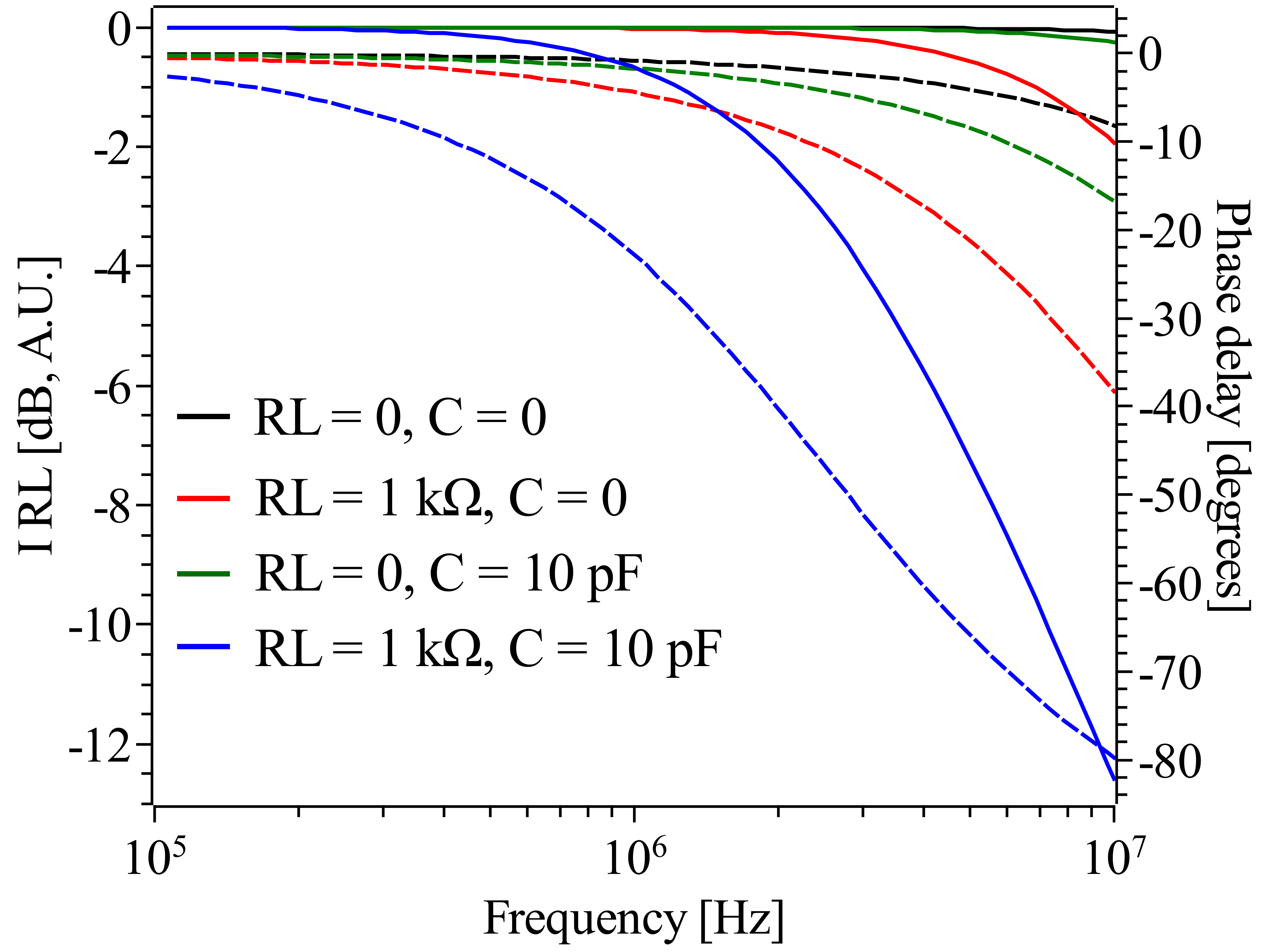
- Margin of electrical stability under various load conditions
- Slew rate
- Power supply rejection ratio
- Thermal stability of quiescent currents
- Open-loop linearity
Ultimately, the main design goals of the amplifier described here are: low-noise, low distortion, fast slew rate and good margin of electrical stability. It must be noted that the average human ear can not identify the distortion content of sound for distortion values below about 1%. In addition, typical distortion values of a speaker are of the order of 1%. For these reasons the pursuit of very low distortion audio amplifiers is usually of academic interest rather than of practical importance. Nothing more will be mentioned regarding topics of an audiophile nature.
Amplifier design methodology
Open-loop non-linearity can be minimised to some degree, however, the inherent non-linearity of transistors and other components prevent a high degree of open-loop linearity. Also, load impedances usually have a frequency dependence and a possible degree of non-linearity. Therefore, the design of a low distortion amplifier mandates the implementation of a negative feedback circuit. A negative feedback circuit with a large loop gain minimises the impact of both non-linearity and noise sources by correcting for the effects of these perturbations. Take into consideration Fig. 1, which is a block diagram of a negative feedback system that consist of linear sub-systems H(s) and F(s). $V_{d}$ is a disturbance voltage which represents the effects of non-linearity or electrical noise.
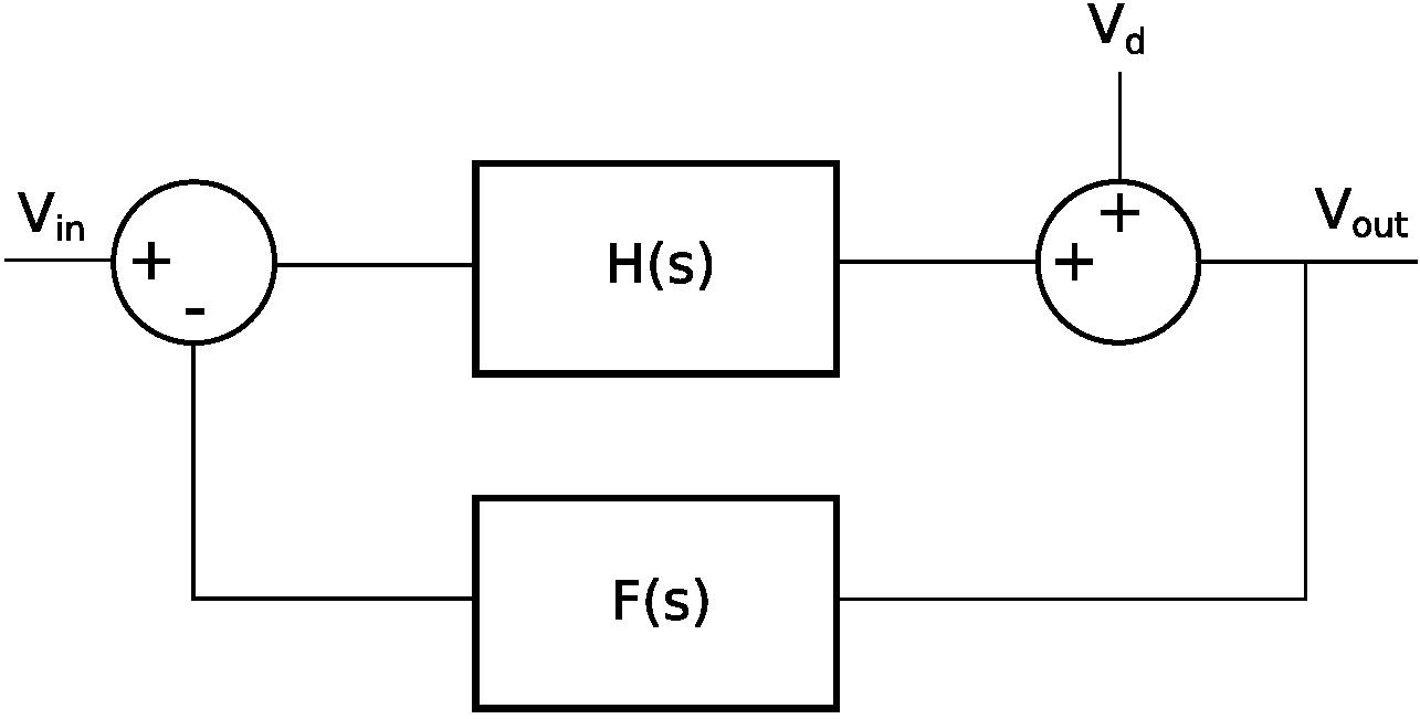
Considering the influence of $V_{d}$, there is a change in the output voltage which is dependent upon the loop-gain,
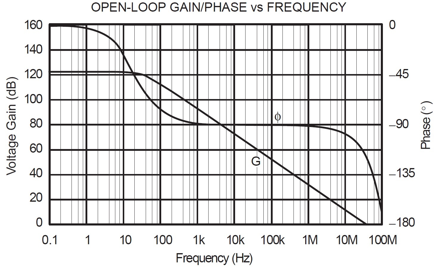
The disturbance voltage, $V_{d}$, can be considered to be the result of noise or non-linearity. In either case the output voltage will reproduce the input voltage to a high degree of fidelity provided the loop-gain, $H(s)F(s)$, is large. As a consequence of the feedback equation, the noise of an amplifier is usually dominated by the noise of those sources that fall outside of the loop, i.e. the input components. The noise characteristics of the amplifier described in this report are measured and analysed in the characterisation section. Another consequence of the feedback equation is the weak dependence of the closed-loop gain, A, on frequency, \begin{equation} \textrm{A} = \frac{V_{\textrm{out}}}{V_{\textrm{in}}}=\frac{H(s)}{1+H(s)F(s)} \end{equation} provided $\textrm{H(s)F(s)}»1$, and the feedback function, $\textrm{F(s)}$ is independent of frequency, which is usually the case where $\textrm{F(s)}$ is simply a voltage divider consisting of resistors. The above equations suggest the cascading of several amplifier stages such that a huge open-loop gain is achieved, thereby, a low-noise, low distortion amplifier will result. However, the electrical stability of a negative feedback circuit needs to be ensured, otherwise it may oscillate or have excessive amounts of overshoot. The stability of a negative feedback circuit is dependent on both the loop-gain and phase delay. With increasing frequency the loop phase delay inevitably increases and the loop-gain decreases. A condition for stability is a loop-gain, $\textrm{H(s)F(s)}$, of less than 1 at the frequency where the phase delay has increased to 180 degrees. The frequency at which the loop-gain decreases to unity is defined as the cross-over frequency, $\omega_{c}$, and the phase margin is defined as $180-\phi_{delay}(\omega_{c})$. As an example see Fig. 2 which is a plot of gain and phase of the OPA350 opamp which is unity gain stable since the phase delay is about 120 degrees (phase margin of 60 degrees) at the cross-over frequency of 38 Mhz.
Stabilisation of an amplifier is usually achieved by including a compensation capacitor which reduces the amplifier gain with increasing frequency such that at the crossover frequency the phase margin is somewhere about 50 degrees or more. A high-performance amplifier has a large loop-gain for the frequencies of interest, and therefore the crossover frequency should be relatively high so that the gain of the amplifier is not excessively curtailed by the action of the compensation capacitance within the frequency band of interest. As a consequence of the necessity of electrical stability, adding an arbitrarily large number of gain stages to an amplifier is not a strategy that produces good results since this will result in excessive phase delay. A larger phase delay requires a smaller cross-over frequency to maintain stability. Therefore, the gain within the audio band will be excessively limited by the compensation capacitance.
Miller capacitance
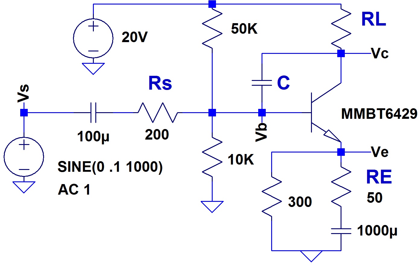
Before discussing the amplifier schematic the effect of miller capacitance will be quantified since it has a considerable impact upon amplifier design and performance through the phase delay that it induces. Referring to Fig. 3, and labelling the AC component of the voltages, \begin{eqnarray} v_{s}(t) = V_{S}e^{i\omega t}\\ v_{b}(t) = V_{B}e^{i\omega t}e^{i\phi_{B}}\\ v_{e}(t) = v_{b}(t)\\ v_{c}(t) = V_{C}e^{i\omega t}e^{i\phi_{C}} \end{eqnarray} the output voltage, $v_{c}(t)$, as a function of frequency is, \begin{equation} v_{c}(t) = v_{S}(t)\frac{-R_{L}\left(\frac{\beta}{\beta+1}\frac{1}{R_{E}}-i\omega C\right)}{1+\frac{R_{S}}{R_{E}}\frac{1}{\beta+1} - i\omega\left[R_{L}C\left(1+\frac{R_{S}}{R_{E}}\right)+R_{S}C\right]-2\omega^{2}C^{2}R_{L}R_{s}} \end{equation} For the above equation it is assumed that the transistor has a finite current gain, $\beta$, but is otherwise ideal and has an infinite frequency response. As such, the miller effect and frequency response is modelled by the external capacitor, C as shown in the schematic of Fig. 3. For small $\omega$, \begin{equation} v_{c}(t) = -v_{s}(t)\frac{\frac{\beta}{\beta + 1}\frac{R_{L}}{R_{E}}}{1 + \frac{R_{S}}{R_{E}}\frac{1}{\beta + 1}} \end{equation} For $\beta»1$ and $R_{S}«\beta R_{E}$ the gain is closely described by the familiar relationship, $R_{L}/R_{E}$. The cut-off frequency is, \begin{equation} \omega = \frac{1}{R_{L}C\left(1+\frac{R_{S}}{R_{E}}\right)+R_{S}C} \end{equation} If $R_{L}»R_{E}$, i.e. the single transistor has significant low-frequency gain the cut-off is approximately inversely proportional to the voltage gain multiplied by the capacitance and input resistance, $R_{S}$. The phase delay is, \begin{equation} \phi=\tan^{-1}\frac{\omega R_{L}C\left(\frac{1}{R_{E}}\left(R_{L}\left(1+\frac{R_{S}}{R_{E}}\right)+R_{S}\right)+2\omega^{2}C^{2}R_{L}R_{S}-1\right) }{\frac{R_{L}}{R_{E}}\left(1+\frac{R_{S}}{R_{E}}\frac{1}{\beta}-\omega^{2}C^{2}R_{L}R_{S}\right)+R_{L}\omega^{2}C^{2}(R_{L}+R_{S})} \end{equation} Taking the 1st order $\omega$ terms the above equation approximates to, \begin{equation} \phi = \tan^{-1}\omega C\left(R_{L}\left(1+\frac{R_{S}}{R_{E}}\right)+R_{S}\right) \end{equation} The bandwidth of the single transistor amplifier is determined by $C$, which is transistor dependent, the voltage gain and input resistance, R$_{\textrm{S}}$. The important point to note is the phase delay increases with increasing voltage gain and input resistance. It is important to consider the phase properties of the voltage amplification stage of an amplifier and eliminate any unnecessary voltage amplification of all other stages. SPICE simulations of the single transistor amplifier shown in Fig. 3 with and without additional external capacitance are plotted in Fig. 4, demonstrating the impact of voltage gain on phase delay and bandwidth. The MMBT6429 transistor is a small signal type with a gain-bandwidth in excess of 300 MHz under the bias conditions of the simulations, however, the phase delay is 38 degrees at 10 Mhz for a voltage gain of 23.3 (red trace).
Amplifier Schematic description
The schematic of the amplifier as constructed and characterised is shown in <a href=”#05_amp_schematic>Figure 5</a>. It consists of four stages, two differential, an output driver, and output stage. The differential gain stages operate in a transconductance mode, i.e. neither are required to generate a significant voltage signal, rather, they are viewed as producing a current signal in response to a small magnitude input voltage signal. The output driver stage consisting of transistors KSA1220A (Q19) and KSC2690A (Q21) is the voltage amplification stage (VAS) and the output stage is a unity gain buffer. C16 (47 pF) connected between the output and the 1st differential stage output is the compensation capacitance. The closed-loop gain is 27k/(470$\times$2) = 28.7 = 29 dB, hence, full-power (50 W into 8 $\Omega$) corresponds to input voltages of 700 mV RMS.
The first differential stage incorporates a current mirror which allows straight forward coupling to the 2nd stage input. In addition, the current mirror doubles the transconductance of the 1st stage and hence the low-frequency open-loop gain. Both differential stages are biased by constant current sources and the quiescent current of the 2nd differential stage biases the output driver stage which in-turn biases the output transistors. Therefore, the quiescent current of the 2nd differential stage determines the quiescent current of the output driver stage. Hereafter, the quiescent currents of the 1st differential, 2nd differential, output driver and output stages are labelled $I_{1}, I_{2}, I_{D}, $ and $I_{O}$ respectively. The two constant current sources of the 2nd stage are assumed to be near equal in magnitude. These constant current sources are adjusted by trimmer potentiometers (R21 and R28) such that $I_{D}$ is set to a desired value.
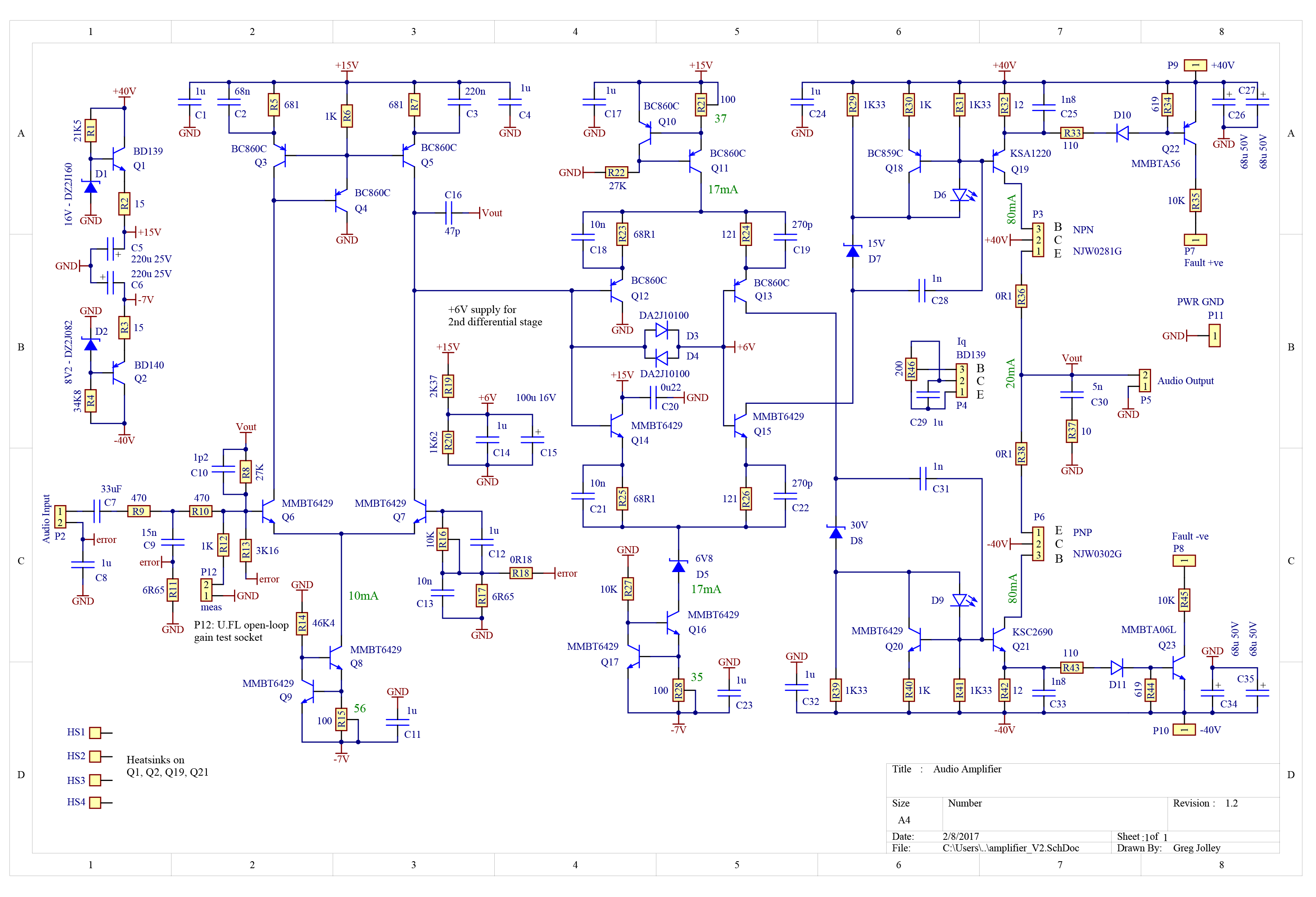
$I_{O}$ is limited by a BD139 transistor placed across the bases of the output transistors. The BD139 should be in close thermal contact with the output transistors so that there are minimal variations to the relative $V_{BE}$ across temperature, therefore, the sensitivity of $I_{O}$ to temperature change is minimised. The sensitivity of $I_{O}$ to temperature has been measured, see the characterisation section.
The two differential stages operate from supply voltages that are different to that of the VAS and output stage. These supply voltages are generated by zener diode based reference voltages that are buffered by transistors. The positive and negative supplies have nominal voltages of 15V and -7V respectively. Separate supplies keep the thermal dissipation of the differential stage transistors to within acceptable limits, reduces voltage stress and broadens the set of transistors that can be utilised by the differential stages.
The input is filtered by a simple RC network (R9, C9) which serves two purposes; firstly it attenuates frequency components of the input signal that lie beyond the upper end of the audio band, secondly it blocks high frequency signals on the input that originate from radiated emissions. The second point is important since a possible amplifier oscillation mode results from the emission of EM radiation via the output cabling, which is picked up by the input cabling. Therefore, the simple RC network may be required to prevent high-frequency oscillations.
Ground currents have the potential to induce hum on the amplifier output, an issue that may be the result of a poor PCB layout. The amplifier input is driven by a separate control board which contains a volume control I.C. (PGA2311). If ground currents produce a small potential difference between the ground planes of the amplifier and control boards, this will result in hum since the control board output signal is with respect to a potential that is slightly different to the amplifier ground potential. The amplifier contains input circuitry which essentially eliminates the possibility of the above mentioned source of hum. The ground potential of the control board is feed into the inverting input of the amplifier, and a portion of it which comes from the R17, R18 voltage divider is feed into the non-inverting input. As such, any ground potential differences do not result in an amplifier output voltage with respect to its ground potential.
As mentioned previously, maintaining a large gain within the audio band while minimising phase delay is a necessary requirement for the design of a high performance amplifier. The amplifier phase delay is minimised about the unity loop-gain point through 2 main mechanisms; the minimisation of the miller capacitance effect and the phase lead resulting from capacitors placed within the second differential stage and the output driver transistor emitter capacitance. C2 and C3 of the 1st differential stage increase the open-loop gain at about 10 kHz. The impedance ratio of C3 in parallel with R7 (C3$\parallel$R7) and C2$\parallel$R5 becomes significant at about 10 kHz, therefore the current signal of Q5 is greater than Q3. At higher frequencies the dynamic impedance of the emitter-base junctions of Q3 and Q5 become greater than C3$\parallel$R7 and C2$\parallel$R5, therefore the current signals in the current mirror become more symmetrical. C19 and C22 of the 2nd differential stage increase the phase margin about the cross-over frequency. Likewise, C25 and C33 (output driver stage) improve the phase margin, but to a leaser extent. Miller phase delay is minimised by the direct coupling of the two differential stages and the voltage amplification stage at higher frequencies through C18, C21, C28 and C31.
The 1.2pF capacitor (C10) that is in parallel with the feedback resistor (R8) greatly improves the stability margin of the amplifier. It is expected that the base capacitance of the input transistor, Q6, in addition to any parasitic capacitance induces a phase delay at its base. This contribution to the phase delay can be eliminated by including a small capacitance in parallel with the feedback resistor. The MMBT6429 data sheet indicates that the typical collector-base capacitance is less than 2 pF at V$_{CB}$ = 5 V. Given the small voltage signal on the collector of Q6, the 1.2 pF capacitor must enhance stability primarily because of a generated phase lead.
The quiescent currents $I_{1}$, $I_{2}$, $I_{D}$, and $I_{O}$, have an impact upon circuit performance and stability. Increasing $I_{1}$ increases the open-loop gain across the entire frequency span and increases the slew rate since the transconductance of the 1st stage is proportional to $I_{1}$. The slew rate is ultimately limited by the amount of current that the 1st differential stage can provide to offset the current through the compensation capacitor,
\begin{equation}\label{slew_Eq} \frac{dv}{dt} =\frac{I_{1}}{47\,pF} \end{equation}
Since the 2nd differential stage requires little input current (in comparison with $I_{1}$), even when the output is driving a large voltage across an 8 $\Omega$ load, the actual slew rate is expected to be close to the value given by the slew equation. For $I_{1}=10$ mA this equates to a slew rate of 213 V$/\mu s$. Essentially, $I_{1}$ should be set to larger values provided stability is not compromised. The phase delay of the driver stage is dependent on $I_{D}$ since the gain-bandwidth product of Q19 and Q21 peak at a particular value of $I_{C}$ and the collector-base capacitance has a dependence on collector current. It is found that $I_{D}$ = 80 mA is a good compromise between minimising phase delay without setting an excessive quiescent current. Through SPICE simulations it is found that reducing $I_{D}$ increases the phase delay around the cross-over frequency while having less impact upon the open-loop gain, therefore the phase margin decreases. There appears to be no point to setting $I_{O}$ beyond a small value. When both output transistors are conducting the transconductance of the output stage is double that of when only a single transistor is conducting. Transitions between these two transconductance modes is a source of distortion.
The open-loop gain and phase, hence, stability depend upon both the magnitude and phase of the load impedance. Speakers and cabling represent quite an unpredictable load. A common practice is to isolate the speaker load at high frequencies and add an additional load with properties that ensure stability. R37 and C30 result in a resistance of 10 $\Omega$ across the amplifier output at high-frequencies, aiding in stability.
The amplifier incorporates basic speaker short-circuit protection to prevent damage to the output transistors and power supply that may otherwise occur if the output is short-circuited. Q22 and Q23 detect excessive driver transistor current and turn on. These signals are detected by the amplifier control board in the form of a MCU interrupt, resulting in rapid shutdown of the amplifier power supply.
More analytic detail on the amplifier gain is found in the Appendix.
SPICE simulations
The circuit for SPICE analysis is shown in Fig. 6, all references to components in this section are with respect to this schematic diagram and the component values for all simulations are as they appear unless otherwise stated. LTspice was used for all SPICE simulations.
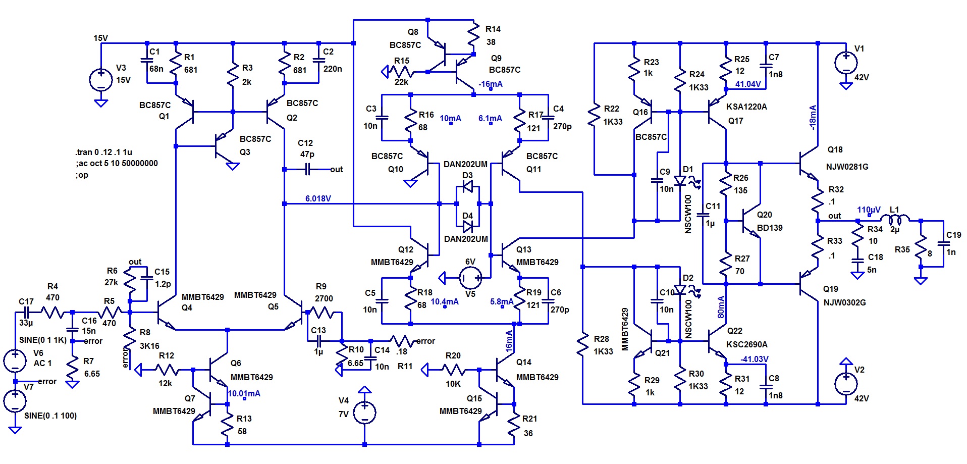
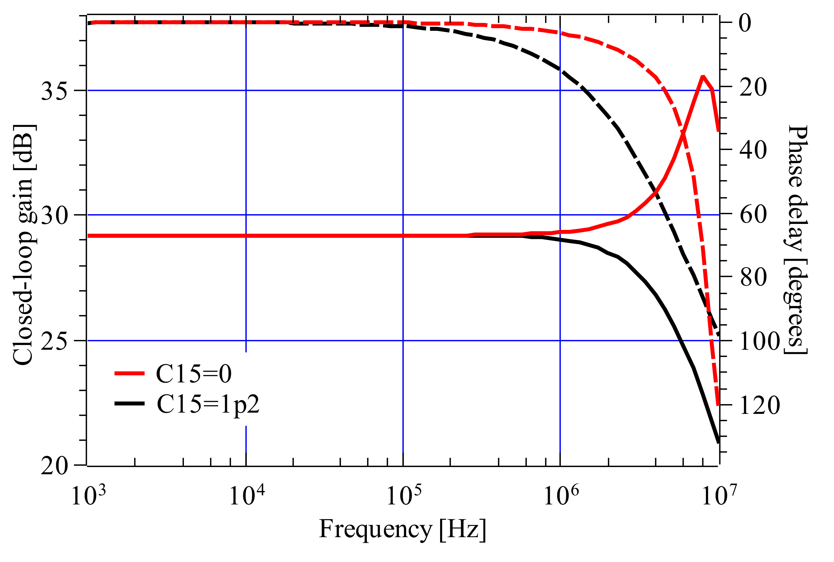
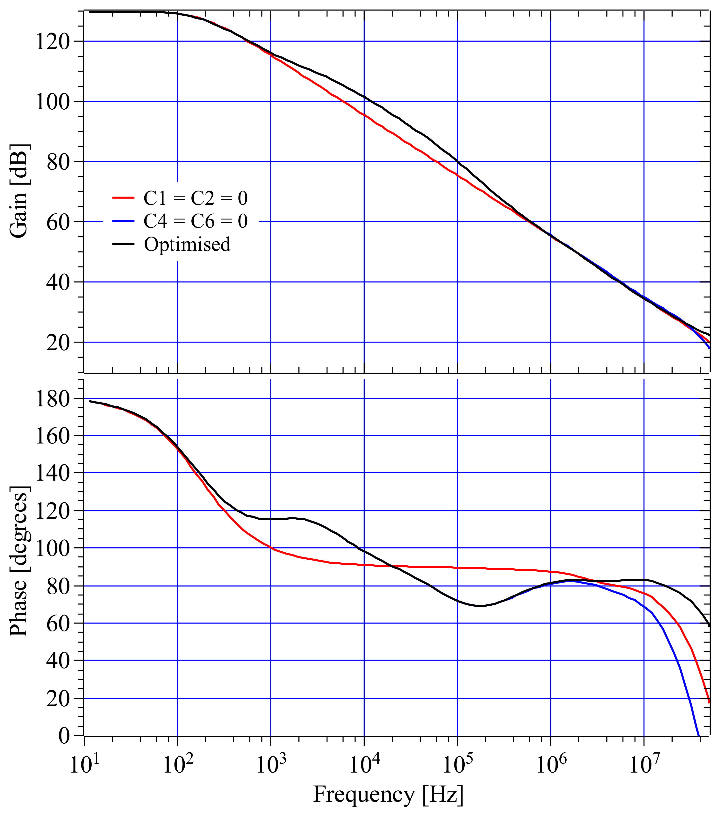
Small signal AC transfer simulations of the closed-loop gain and phase for the optimised component values as shown in the simulation schematic is shown in Fig. 7. In-addition, plots are shown for the feedback capacitor, C15=0. The benefits of C15 are clearly evident by the elimination of gain peaking at about 8 MHz and reduction of the phase delay at about the cross-over frequency. Transient simulations indicate that the full-power bandwidth is a little over 1 MHz.
The open-loop gain and phase for the optimised component values is shown in Fig. 8.
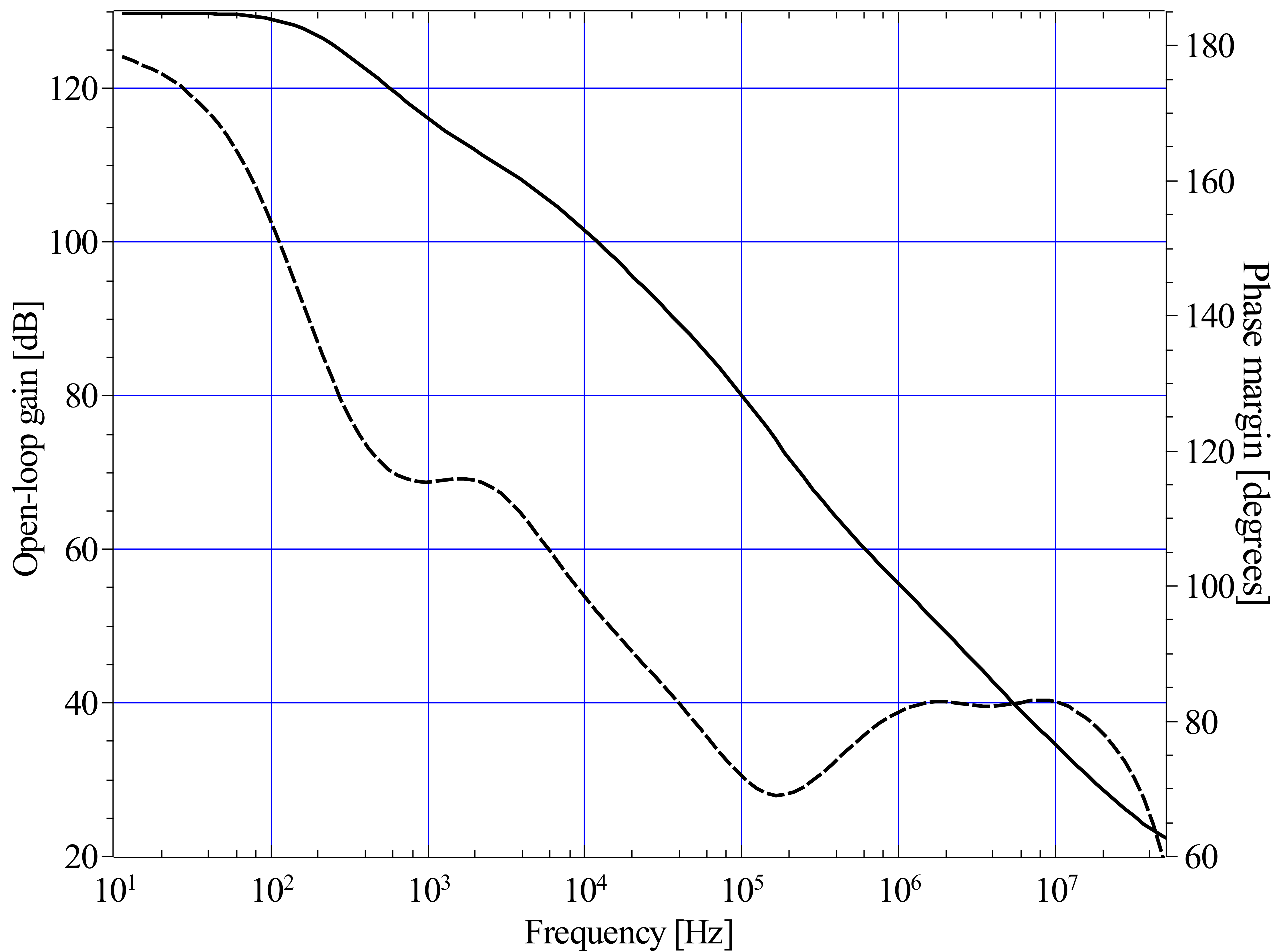
The two differential gain stages results in a very large voltage gain of 130 dB at frequencies less than 100 Hz. The gain reduces with increasing frequency beyond 100 Hz due to the 47 pF compensation capacitor. The reduction of open-loop gain with increasing frequency (aside from the influence of other capacitors such as C1 and C2) can considered as the result of the reduction of the load impedance at the output of the 1st differential stage, \begin{equation} gain \propto \frac{1}{Z}=\frac{1}{\omega\times 47\,pF} \end{equation} which equates to -6 dB per octave. The inclusion of capacitors C1 and C2 pushes the gain at 10 kHz to a little over 100 dB. The cross-over frequency is modified by C16 which increases the closed-loop gain at higher frequencies to 27k/470 = 57 = 35 dB, giving a cross-over frequency a little under 10 MHz and a phase margin of 80 degrees, though the phase margin minimum is 69 degrees at 170 kHz.
The frequency at which the open-loop gain begins to decrease is given by the relationship, \begin{equation} \omega\times 47\,pF \times gm_{2}\times gm_{D}\times rm_{O}= Z_{out_{1} } \end{equation}
Where $gm_{2}$ is the transconductance of the 2nd stage, $gm_{D}$ is the transconductance of the driver stage, $rm_{O}$ is the transresistance of the output stage and $Z_{out_{1}}$ is the impedance as seen at the output of the 1st differential stage. $Z_{out_{1}}$ is the result of the early voltage of Q5 and the load impedance of the 2nd stage input. For more detail see the appendix.
A summary of the peak-peak magnitudes of various signals is shown in table 1 and stage gains are shown in table 2. The voltage gain of the 1st differential stage is given by,
\begin{equation} \frac{\Delta V_{B}Q10}{\Delta V_{B}Q4} \end{equation} The transconductance of the 2nd stage is given by, \begin{equation} \frac{\Delta I_{C}Q11}{\Delta V_{B}Q10} \end{equation} The current gain of the driver stage is given by, \begin{equation} \frac{\Delta I_{C}Q17}{\Delta I_{C}Q13} \end{equation} The transresistance of the output stage is given by, \begin{equation} \frac{\Delta V_{out}}{\Delta I_{C}Q17 + \Delta I_{C}Q22} \end{equation}
It is evident that the gain of all stages apart from the output are largely independent of output magnitude. The transresistance of the output stage depends on the load impedance and current gain of the output transistors which is dependent on $V_{CE}$. The early voltages of the driver transistors have little impact upon the combined transresistance of the driver and output stages due to the emitter resistors, R25 and R31.
| Vout | V$_{B}$ Q4 ($\mu$V) | V$_{B}$ Q10 (mV) | I$_{C}$ Q11+Q13 (mA) | I$_{C}$ Q17 (mA) | I$_{C}$ Q22 (mA) |
|---|---|---|---|---|---|
| 10 | 3.5 | 27.5 | 0.278 | 3.18 | 3.51 |
| 20 | 7.68 | 60.9 | 0.616 | 7.18 | 7.84 |
| 30 | 12.8 | 102 | 1.03 | 12.3 | 13.2 |
| 40 | 19.2 | 153 | 1.55 | 18.8 | 20.0 |
| 50 | 27.3 | 219 | 2.21 | 27.2 | 28.6 |
| 60 | 38.1 | 305 | 3.07 | 38.4 | 40.0 |
| Vout | Av 1st-stage | $g_{m}$ 2nd-stage | A$_{I}$ driver | $r_{m}$ output stage | total open-loop gain (dB) |
|---|---|---|---|---|---|
| 10 | 7860 | 0.0101 | 25.3 | 1490 | 129.4 |
| 20 | 7930 | 0.0101 | 25.5 | 1330 | 128.3 |
| 30 | 7970 | 0.0101 | 25.7 | 1180 | 127.4 |
| 40 | 7970 | 0.0101 | 26.0 | 1030 | 126.4 |
| 50 | 8020 | 0.0101 | 25.9 | 896 | 125.3 |
| 60 | 8010 | 0.0101 | 26.6 | 765 | 123.9 |
Various transient waveforms for a 1 kHz input signal are shown in Fig. 10. What is interesting is the very non-sinusoidal waveforms of the 1st stage output and the base voltage of Q17. It turns out that the rather small early voltages of the output transistors is the primary influence on the shape of these waveforms. As a function of collector current the current gain of the output transistors are very linear, however, the current gain has quite a strong dependence on V$_{CE}$ leading to a output stage transresistance that is non-linear and dependent on the amplifier output voltage. The voltage on the base of Q4 is close to sinusoidal because the compensation capacitance linearises the load on the 1st stage output. Simulations were performed for a 50 Hz sine wave input of several different magnitudes such that the compensation capacitance has negligible influence on the gain. The low-frequency was chosen to investigate the gain of the various stages of the amplifier as a function of output magnitude.

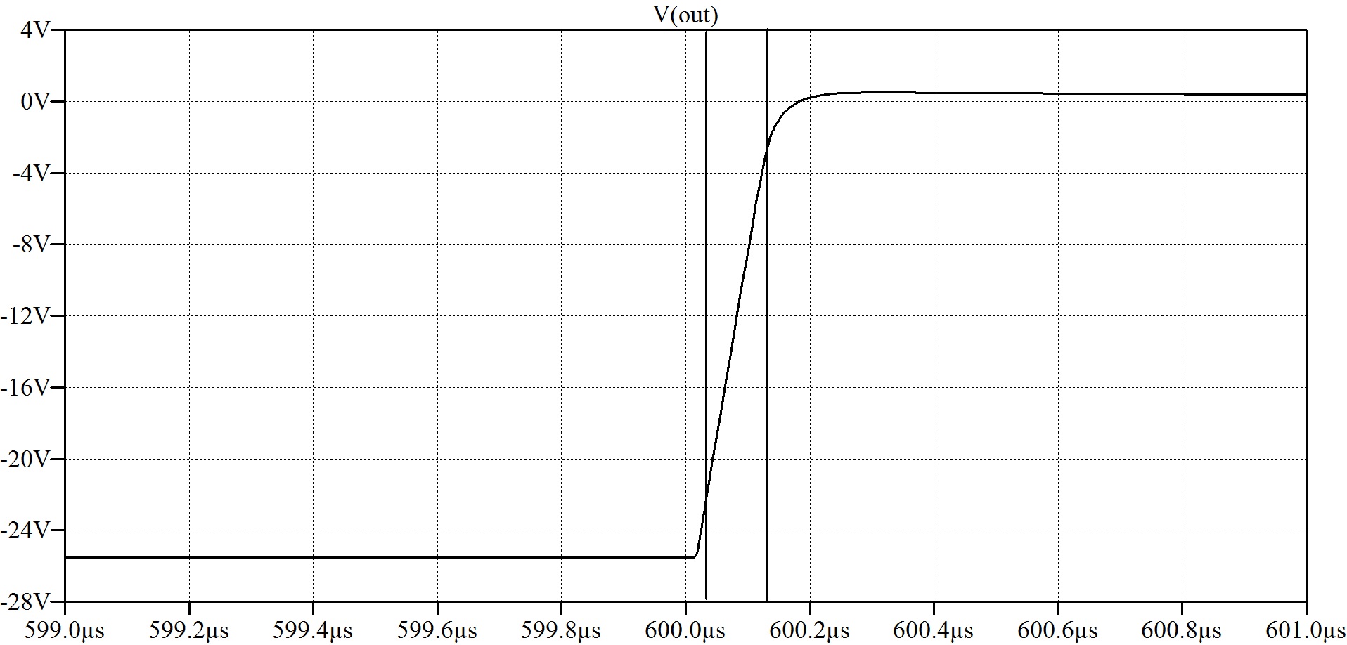
The response to a square wave input with the input filter capacitor (C16) removed is shown in Fig. 11 indicating a slew rate of 230V/$\mu$S which is is close to the upper limit calculated in the amplifier schematic description section.
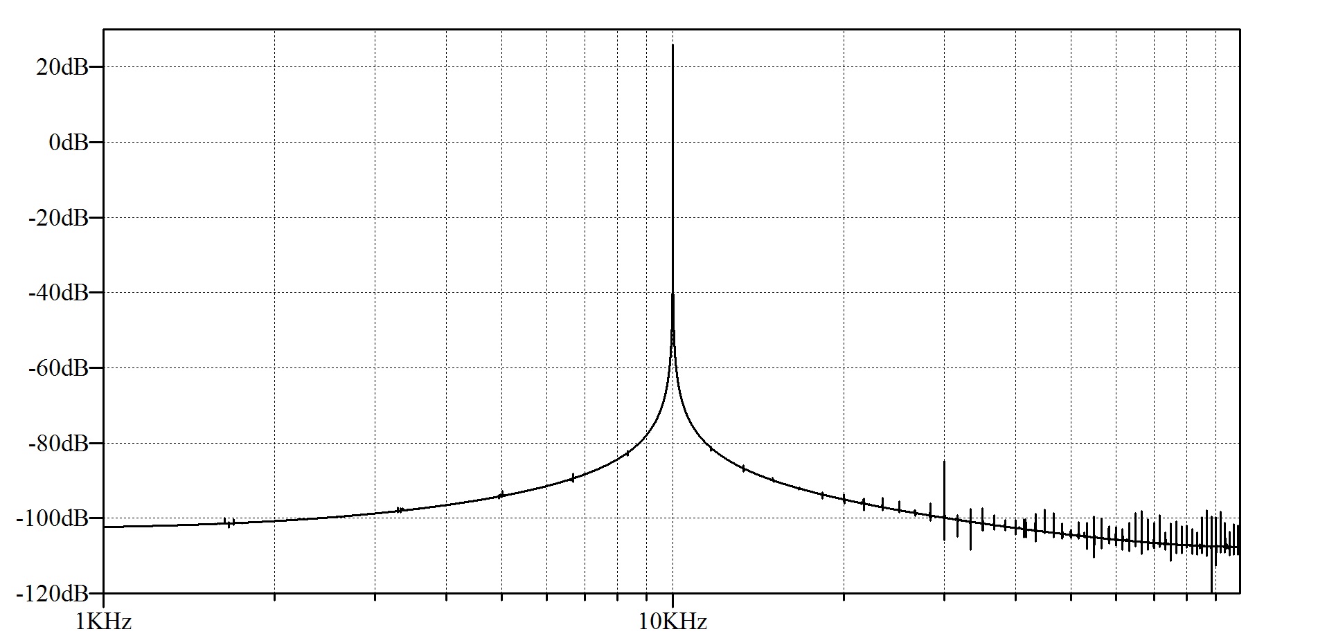
A long transient simulation with a small time-step was performed for a 10 kHz input and a FFT was taken of the output waveform to obtain an indication of the amount of amplifier distortion, see Fig. 12.
Simulations were performed to investigate the dependence of the amplifier output voltage on the error voltage (V7). It was found that there is a negligible output voltage in response to V7 (simulation results not shown).
Component Selection
The components that have a significant impact upon the amplifier performance thought choice of their type are;
- Output transistors
- Output driver transistors
- 1st and 2nd differential stage transistors
Output transistors
NJW0281 (npn) and MJW0302 (pnp) are ideal output stage transistors due to their excellent gain linearity (gain matching within 10\% from 50 mA to 3 A), exceptionally safe operating area and high transition frequency. The high transition frequency and a relatively small output capacitance of 400 pF ($V_{CB}$=10 V) minimises the phase delay at higher frequencies. However, their small early voltage is a significant source of non-linearity.
Output driver transistors
The KSA1220A (pnp) and KSC2690A (npn) are ideal choice as the driver transistors due to their small output capacitance of 19 pF ($V_{CB}$=10 V), large gain, and a gain-bandwidth-product of 155 MHz ($V_{CE} = 5 V, I_{C}$ = 0.2 A).
Differential input pair transistors
MMBT6429 transistors have been chosen for the NPN differential stages due to the following reasons:
- Very large gain
- Gain-bandwidth product of about 350 MHz at 5 mA and V$_{CE}$ = 5 V.
- High Early voltage
- Low-noise
Supply rail decoupling capacitors
The power supply must be decoupled with capacitors that exhibit a low impedance at high frequency otherwise oscillations may result due to an unintentional feedback path. When a load is driven at high frequency, modulation of the supply voltage resulting from a supply impedance may be fed back into the input resulting in oscillations. Both supply rails are decoupled by two 68 $\mu$F polymer electrolytic capacitors, manufacturer part number 50SVPF68M.
Feedback resistors
Common resistor technologies (either thin or thick film) are suitable for the majority of the amplifier resistors. Amplifier noise is dominated by the noise of the input transistors and associated input resistors, therefore there is some motivation for the use of resistors with low excesses-noise.
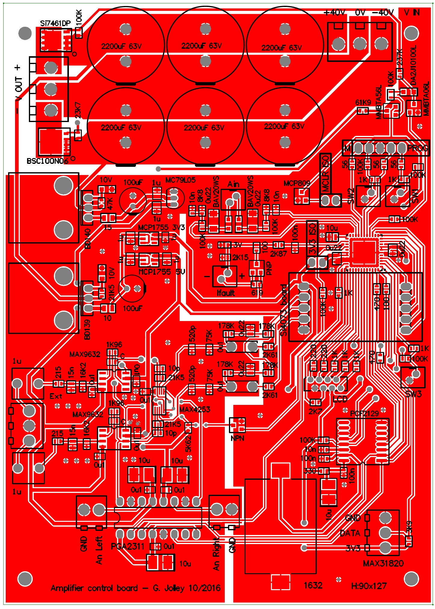
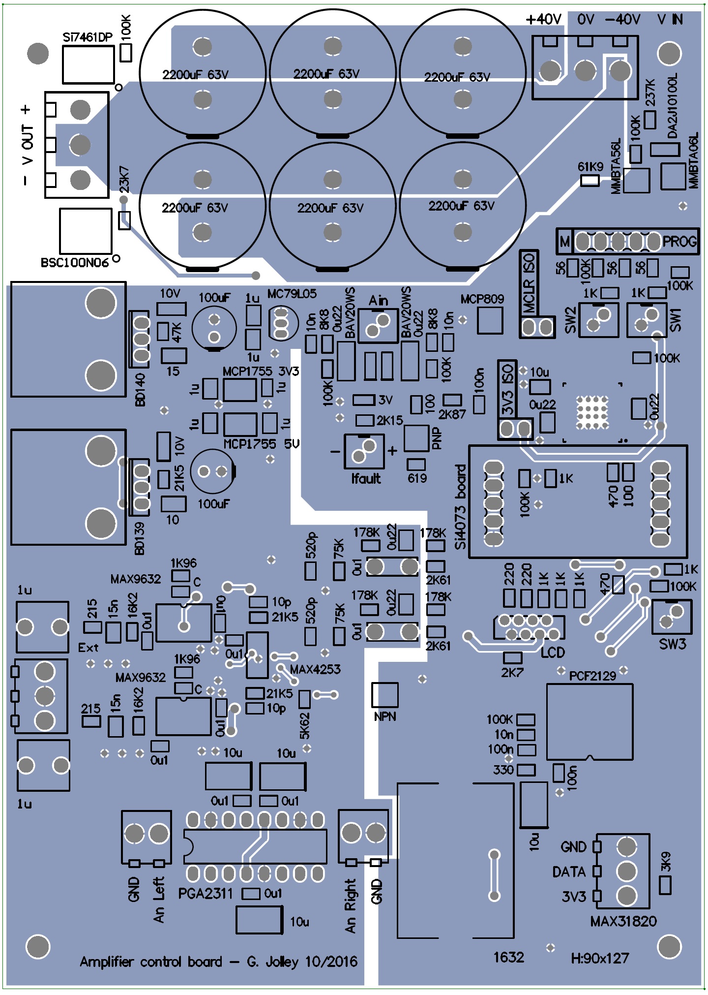
PCB layout
Consideration of the PCB layout is essential since an inadequate layout can be a major contribution to amplifier hum, electrical instability and distortion. An understanding of the following phenomena is needed in order to design a good layout:
- Inductive coupling - time dependent current loops can induce voltages around other trace loops.
- Capacitive coupling - traces undergoing voltage transitions can induce voltage fluctuations on other traces.
- Ohmic trace resistance - current will induce a voltage drop across a trace.
- Parasitic inductance and capacitance - can result in an unintentional impact upon the magnitude and phase of analog signals.
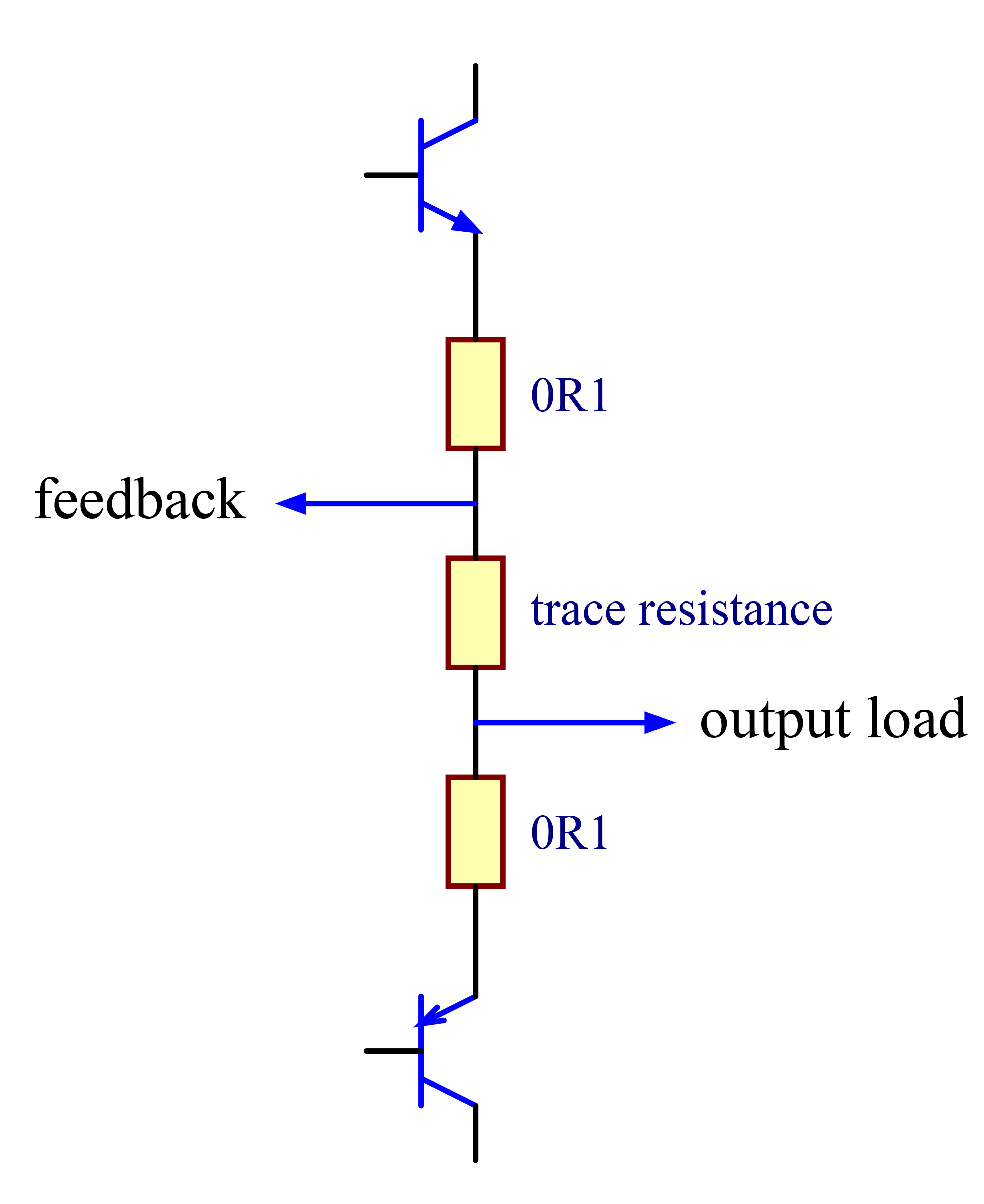
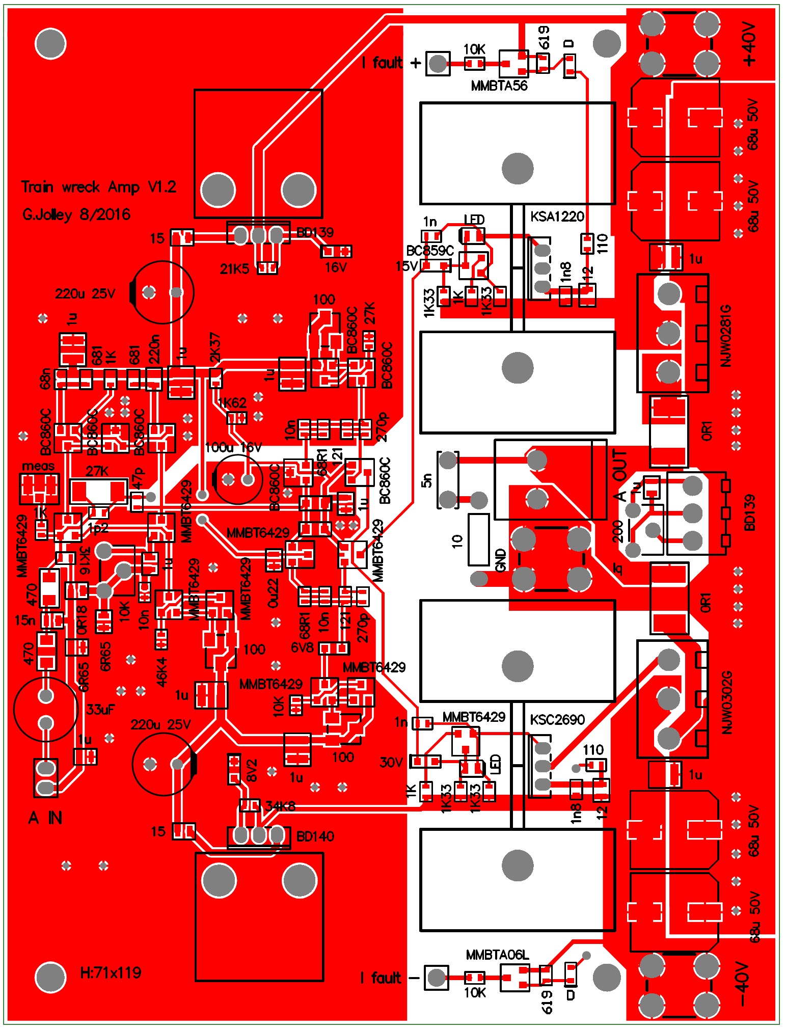
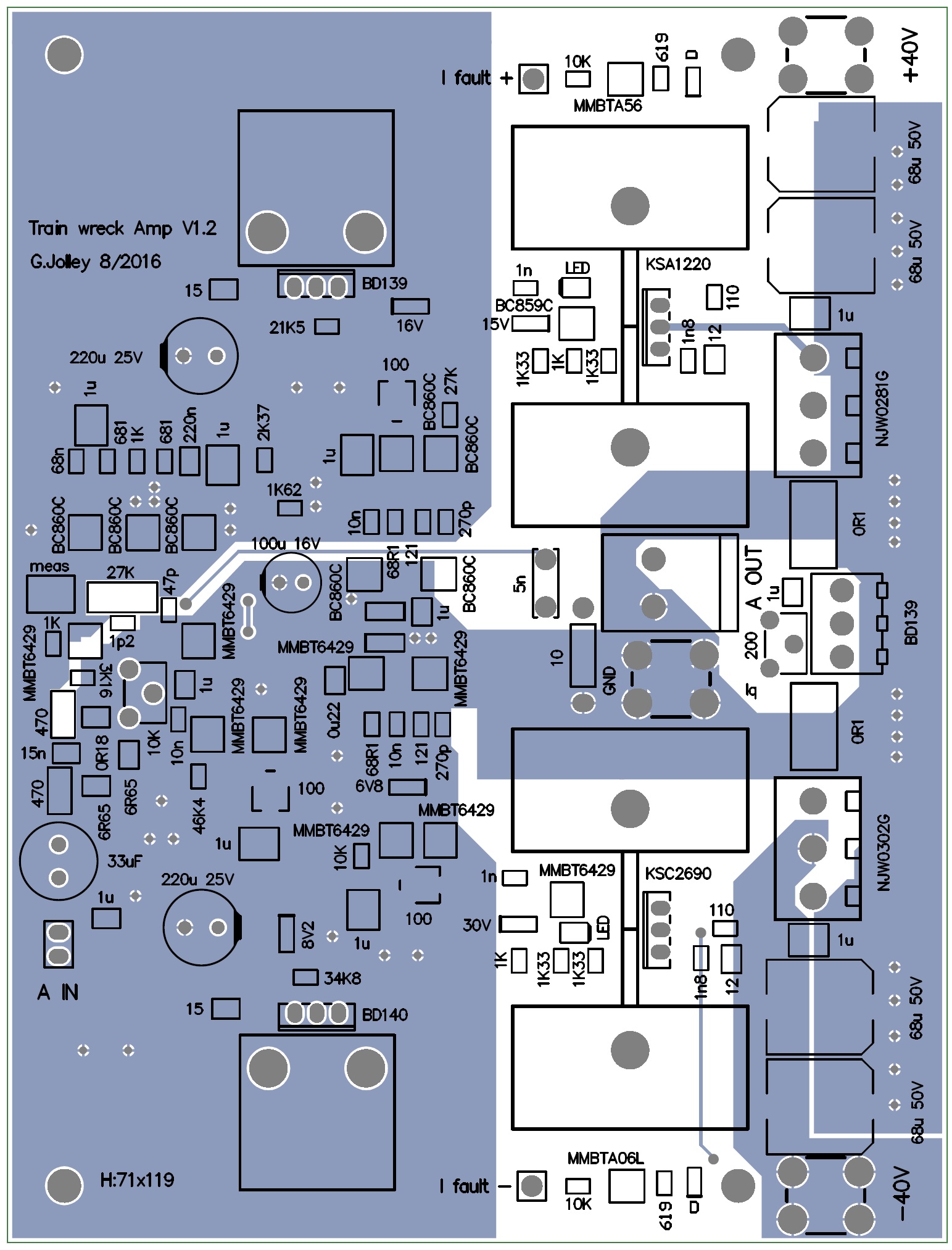
At worst, inductive coupling can result in unintentional feedback paths pushing the amplifier into an unstable electrical state and otherwise can be a significant source of distortion and noise. Wires and traces carrying the large currents that drive the output load should be inductively isolated from the small signal differential stages. Isolation can be achieved through distancing the differential stages from large current loops and by the use of a ground plane to shield the input stages. In addition, minimising trace length and the area of current loops will minimise inductive coupling. Similar techniques minimise the impact of capacitive coupling between the input and output stages of the amplifier. Fig. 13 is a diagram of an output stage and depicts a potential impact that trace resistance can have on amplifier distortion. The feedback trace is not directly connected to the output and the asymmetry leads to a predominantly 2nd order harmonic content. A little bit of trace resistance may seem trivial, however, a simple calculation suggests that the impact can be greater than expected. Consider the case where the feedback trace is isolated from the output by a trace of length 3 cm with a width of 5 mm resulting in a trace resistance of about 3 m$\Omega$ (1 oz/ft$^{2}$). For a load impedance of 8 $\Omega$ driven by a peak voltage of 24 V (load current 3 A) this results in a feedback error voltage of 9 mV between the positive and negative voltage cycles. 9 mV in 24 V is 0.0375% and, therefore, possibly the greatest source of distortion in an amplifier! The potential impact that parasitic capacitance can have on the feedback phase can be calculated by considering the case of the feedback trace (length 6 cm, width 0.3 mm) running over a ground plane. For a PCB thickness of 1.2 mm this results in a capacitance of 2.8 pF. If the feedback resistor (27 K$\Omega$) is placed directly at the output this results in an additional phase delay of about 4.6 degrees at 10 MHz. The top and bottom copper layouts are shown in figures 14 and 15. The high current output stage is isolated from the input sections and no large ground current loops influence the input sections.
Amplifier characterisation
Electrical stability
The electrical stability of the amplifier as a function of $I_{1}$, $I_{2}$ (hence $I_{D}$) and $I_{O}$ was experimented with and the stability was found to be excellent. As explained in section description, the open-loop gain across all frequencies, and therefore, stability depend on $I_{1}$. Therefore, stability can be examined by performing measurements as a function of $I_{1}$, in particular the response to a square wave input. The response to a square wave input with the input filter capacitor (C9) removed showed insignificant overshoot over the current range $I_{1}$ = 5 $\to$ 15 mA.
| Temperature | Current (mA) |
|---|---|
| 29 | 20 |
| 49 | 38 |
| 66 | 58 |
| 89 | 104 |
Thermal stability - quiescent current drift
The output stage quiescent current temperature dependence was measured by driving an $8\,\Omega$ load with a sine wave for a period of time sufficient for thermal steady state. The heatsink temperature and $I_O$ are recorded in table 3. ${I}_{O}$ has a temperature dependence that is a little excessive, a suggestion to address this issue is made in section Future work.
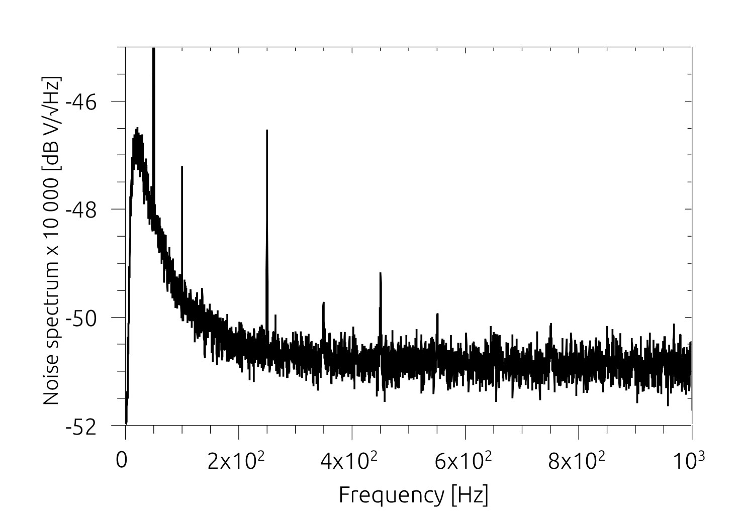
Noise and hum
The output noise of the amplifier was measured over the 20-1 kHz band using a low-noise amplifier with a gain of 10 000 connected to the output. Wide-band noise was measured with the power amplifier connected to a regulated power supply. The low-noise amplifier was connected to a spectrum analyzer (analog discovery 2, Digilent). The noise spectrum obtained with the amplifier input connector, P2, shorted is shown in Fig. 16. The wide-band noise of the amplifier due to the thermal noise of the input resistors is calculated to be, \begin{equation} v_{noise}(RMS) = \sqrt{4k_{B}T\left[725 \left(\frac{27k}{725}\right)^{2}+\frac{1670}{\sqrt{1+(\omega 1670\times 10^{-6})^{2}}}\left(\frac{27k+725}{725}\right)^{2}+27k\right]} \end{equation} where 725 is R9+R10 in parallel with R13, 1670 is the resistance setting of trimmer R16, and $10^{-6}$ is the capacitance of C12. The frequency dependent term becomes significant for frequencies less than about 100 Hz. For frequencies greater than about 200 Hz the calculated noise density due to resistor thermal noise is 131\,\, $nV/\sqrt{Hz}$
The flat band noise of the amplifier is measured to be -51 dB/10000 = 282 nV/$\sqrt{Hz}$. Upon multiplication by the low-noise amplifier gain, the noise spectral density due to resistor thermal noise is calculated to be $-57.7$ dB. The 6.7 dB difference is consistent with the noise figure of the MMBT6429 transistor.
The noise voltage over the 20 Hz - 20 kHz band is about $\sqrt{20000-20}\times 282\,nV$ = 40 $\mu V$ RMS. Note, the peaks at 50 Hz + harmonics originate from EM interference of the low-noise amplifier input cabling.
Open-loop gain
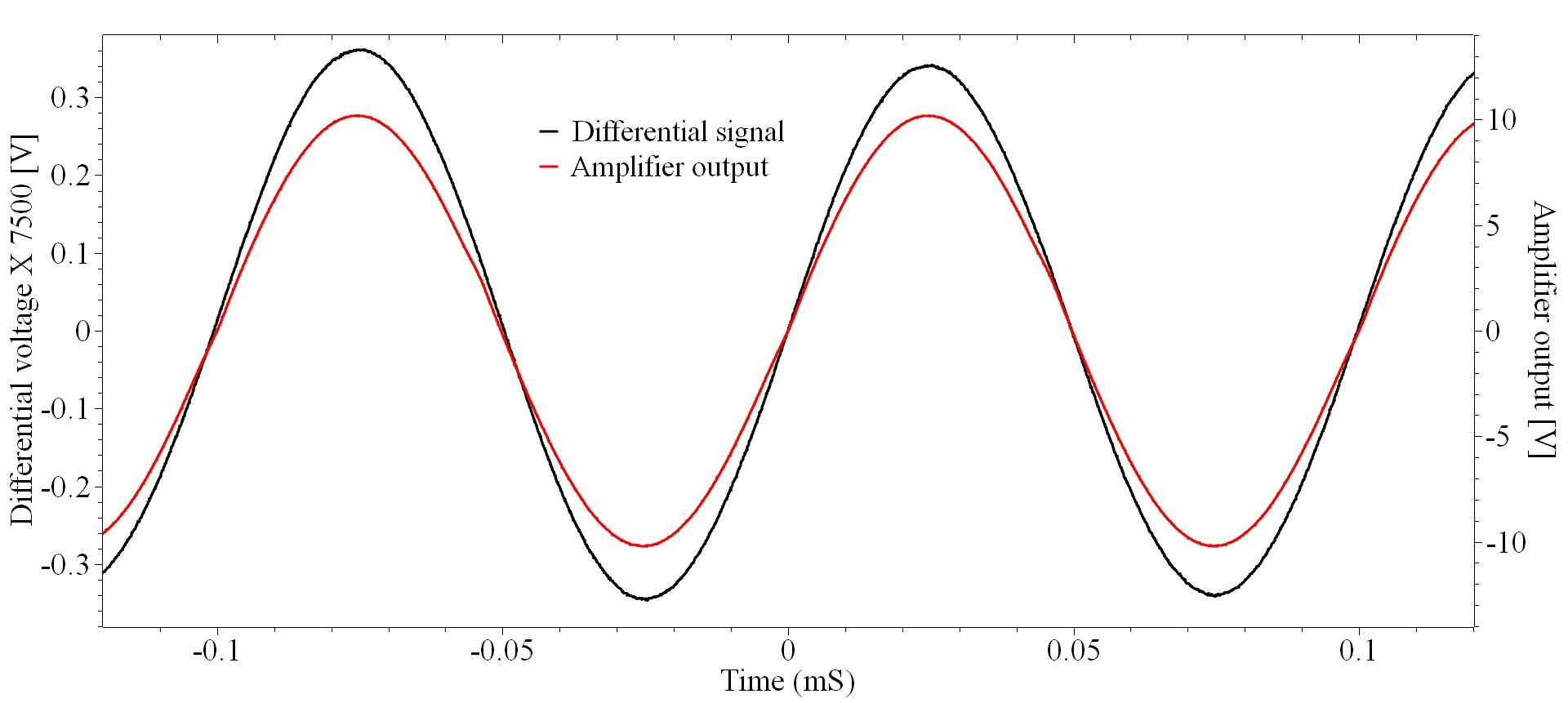
Open-loop gain measurements were successfully performed by connecting a low-noise amplifier with a gain of 7500 to the U.FL test connector of the amplifier board. Waveforms captured with an oscilloscope for a 10 kHz input signal are shown in Figure 17. The measured gain of 106 dB compares quite well with the calculated value of 102 dB. At 1 kHz the measured gain is 113 dB and the calculated gain is 116 dB.
Slew rate
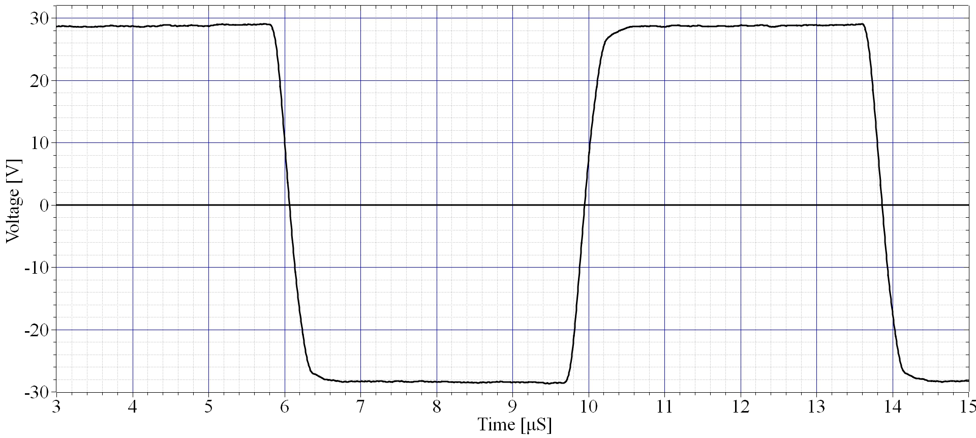
Slew rate measurements were performed by injecting a square wave into the input with the filter capacitor (C9) removed. The output waveform is shown in Fig. 18 indicating a slew rate of about 130 V/$\mu S$. This value is significantly less than the calculated slew rate, the difference is attributed to the rise time of the square wave oscillator.
Distortion measurements
Work is in progress to design and construct circuitry capable of measuring low levels of distortion.
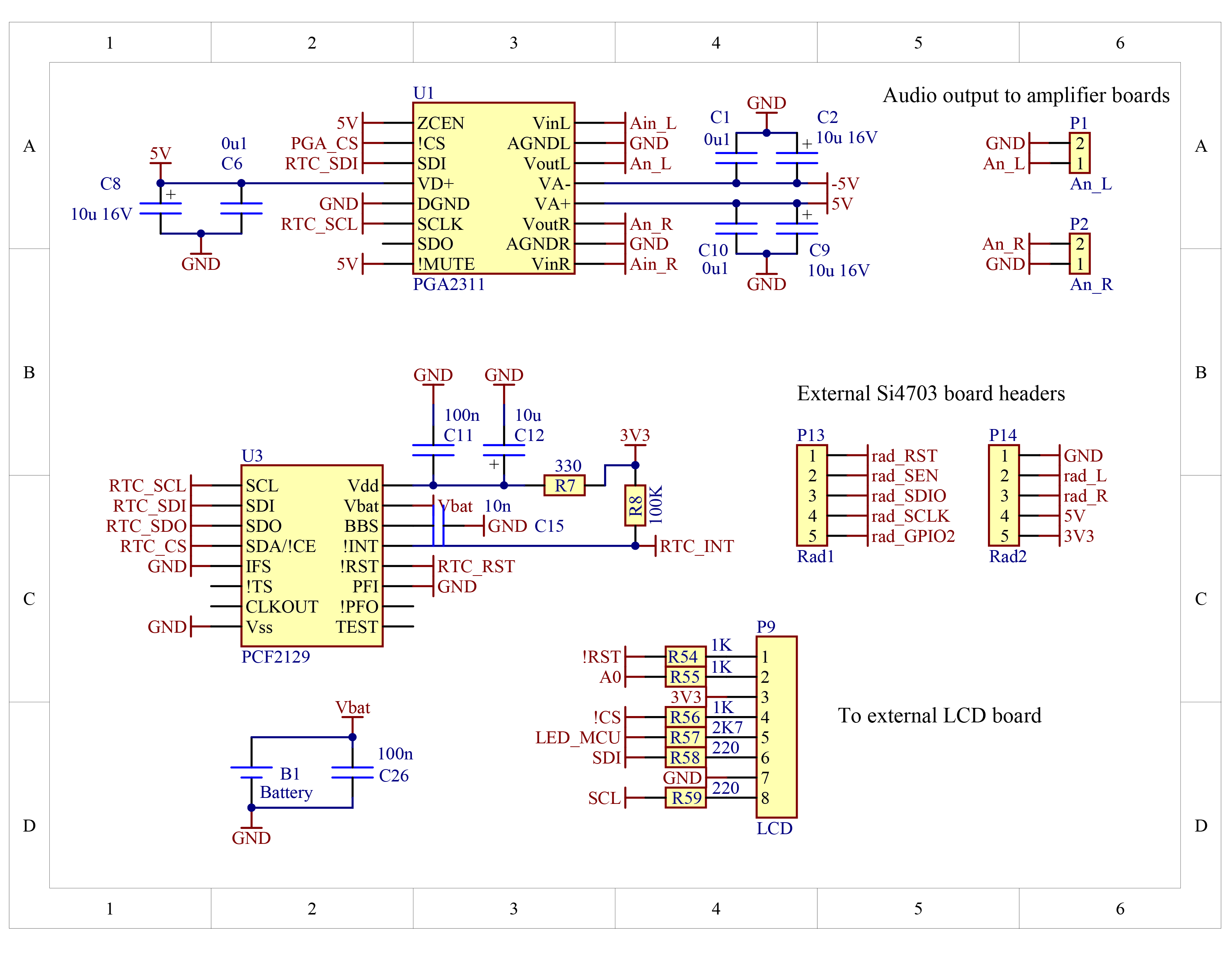
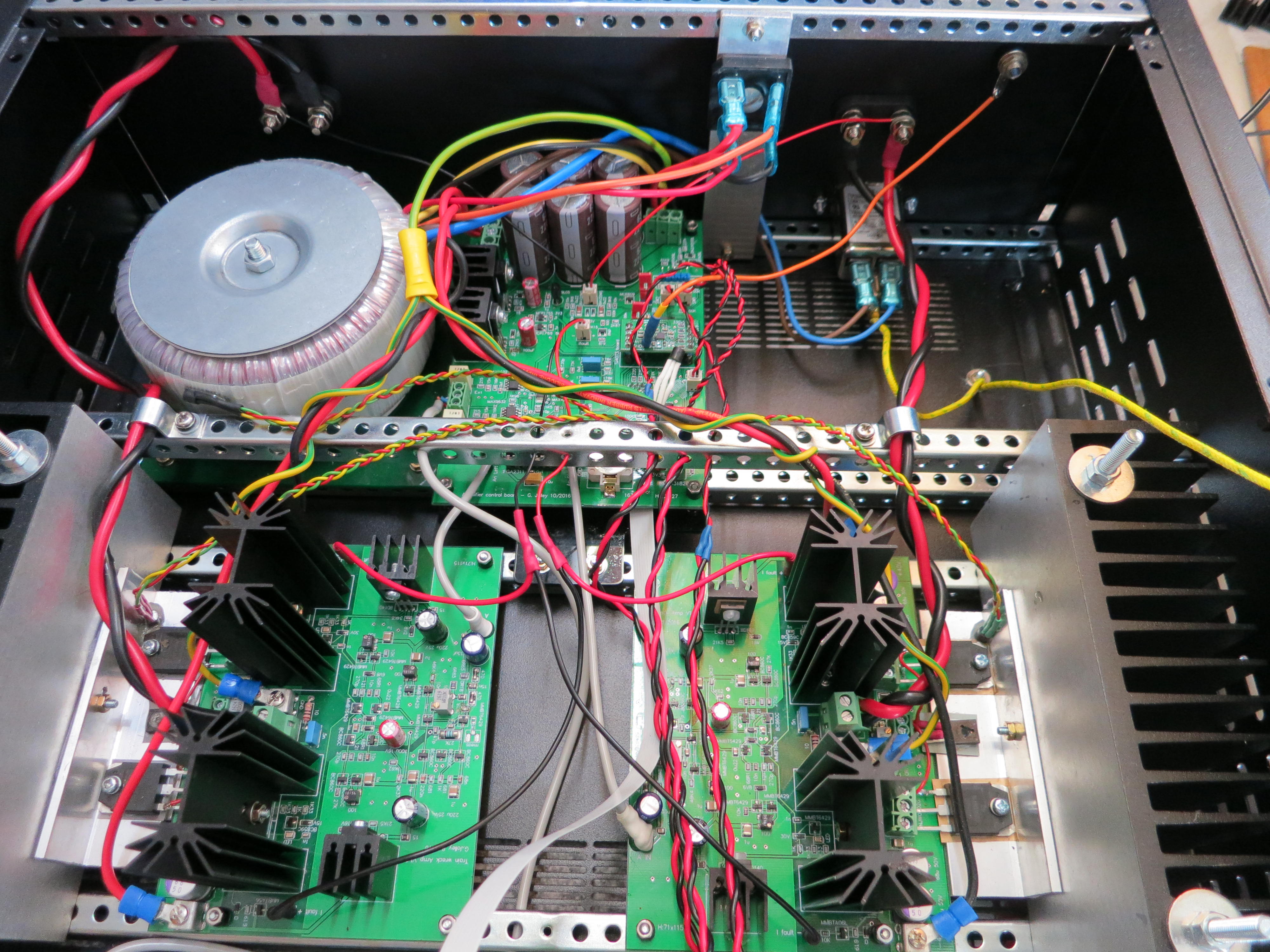
Control board
At a minimum an amplifier of more than minimal cost should be immune to catastrophic damage under the event of an output short-circuit or excessive thermal stress. These requirements can be effectively implemented by a cheap microcontroller circuit. Considering the overall cost of the amplifier which is dominated by the transformer, heatsinks, output transistors and case etc, from a design and component cost perspective there is motivation to add functionality to an amplifier which is of relatively low cost. A control board which protects the amplifier from short-circuit and thermal faults and includes radio, alarm clock, and volume control functionality has been designed and constructed and is briefly described below. Incorporating radio and time keeping functionality allows for alarm clock functionality through software development.
Volume control
A PGA2311 I.C. is chosen as the volume control device due to its low-noise and distortion, simple SPI digital interface and ability to drive 600$\Omega$ loads directly. The PGA2311 has a wide gain and attenuation range; +31.5 dB to -95.5 dB with 0.5 dB steps, however, the range that is useful to the amplifier is likely to be +31.5 dB to about -20 dB. It should be noted that the digital supply of the PGA2311 is +5V, however, it is driven directly by the 3.3V I/O pins of the MCU since the data sheet indicates that the minimum high-level input voltage of the PGA2311 is 2V.
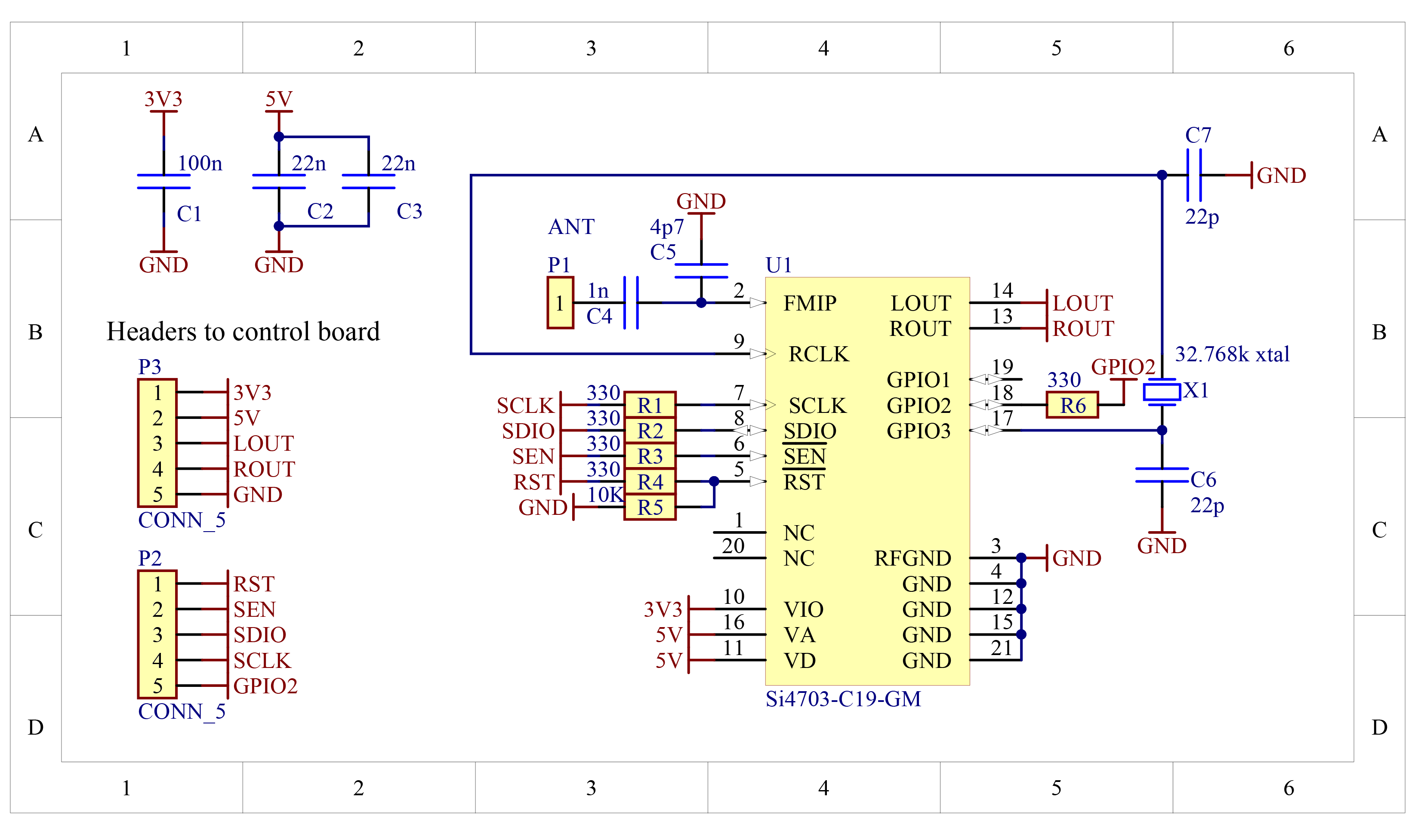
FM radio receiver
A Si4703 I.C. is chosen as the radio receiver due to one feature in particular - it is essentially a complete radio on a chip. It integrates all tuner functions from antenna input to stereo audio output. Basically, when designing the amplifier and control board I was not interested in designing something that required RF techniques. However, the Si4703 is a very attractive option due to its high performance characteristics. Its most significant features are:
- Simple 2 or 3-wire digital interface
- Worldwide FM band support (76–108 MHz)
- Seek tuning
- Automatic frequency control (AFC)
- Automatic gain control (AGC)
- Excellent overload immunity
- Signal strength measurement
- Programmable de-emphasis (50/75 $\mu$s)
- Adaptive noise suppression
- Line-level analog output
A separate PCB was constructed for the Si4703 which plugs into the control board.
Real-time clock
A PCF2127 I.C. is chosen as the time keeping device. Its most notable feature is an integrated temperature compensated crystal oscillator. It incorporates a host of features that are not utilised by the control board, however, it is included in the control board since I intend to use it for other projects as such the PCF2127 software I write for the control board will be reused later.
Temperature sensors
MAX31820 sensors are chosen as the amplifier temperature monitoring devices. An attractive feature of these devices is their 1-wire interface which reduces MCU pin count requirements and PCB routing requirements.
Display
The NHD-C12864LZ-FSW-FBW-3V3 LCD is chosen as the display device since it has sufficient resolution (128 X 64) to display the volume, temperature, radio and clock parameters, has an LED back-light and has an appropriate active area. Also, this LCD can operate from a SPI port which reduces the MCU pin count requirements.
MCU
The PIC18F47J13 is chosen for the microcontroller device for reasons that include:
- It is a simple 8-bit MCU which simplifies the writing of code
- A MCU with a small computational throughput is ideal for the control device
- Peripheral pin select - simplifies PCB routing
- SPI port with direct memory access - simplifies writing routines for the LCD
- A change in an I/O pin state can trigger an interrupt for interface to the amplifier current fault detection circuit
- Interrupt sources can be assigned to one of two priorities, therefore, a current fault can interrupt any low-priority interrupts that are in service
- An internal ADC allows measurement of the amplifier output voltage
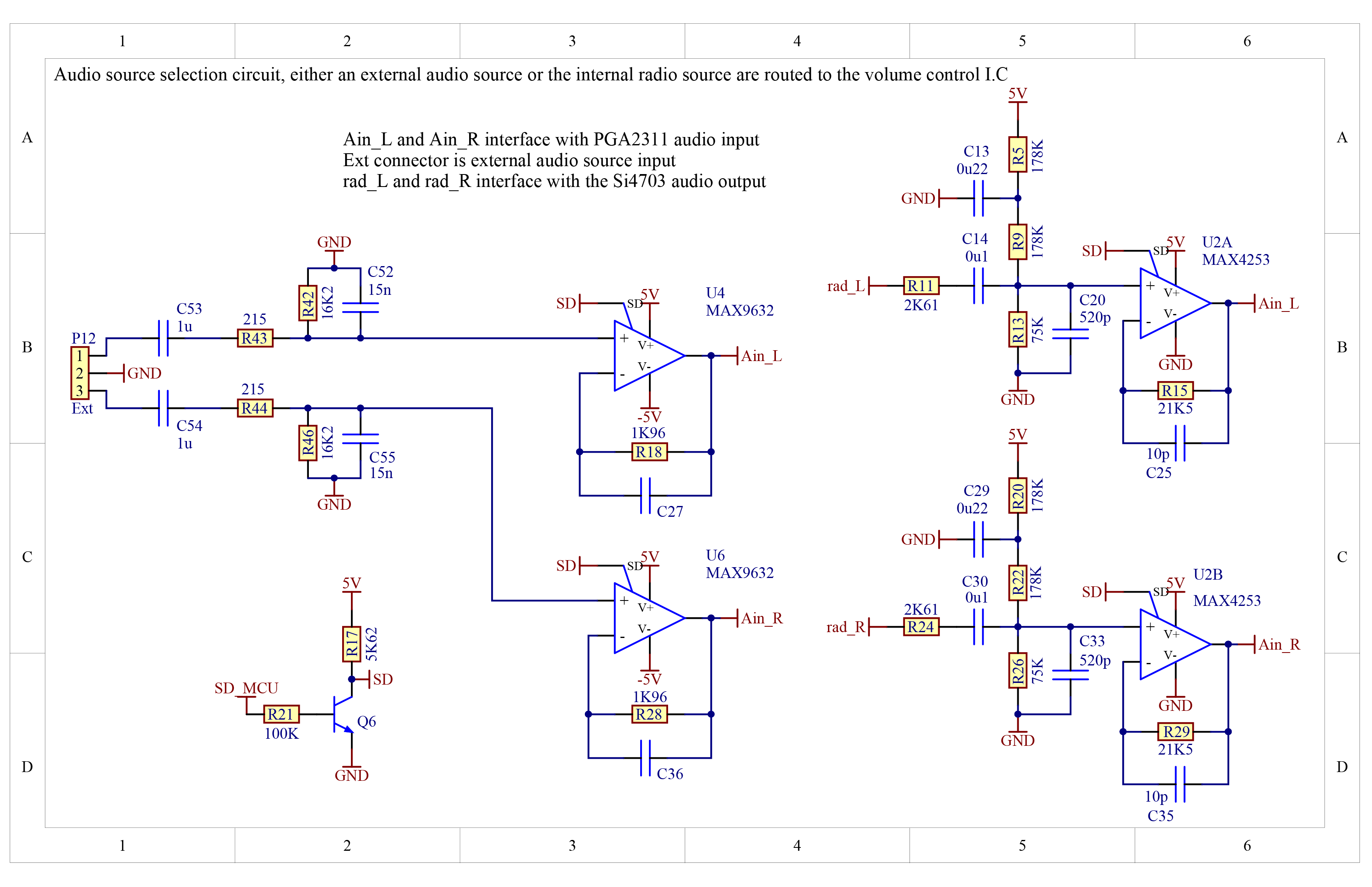
Audio source selection
Circuitry is needed to switch between the Si4703 and external audio sources. This is achieved by the use of opamps with a shutdown feature that puts the output into a hi-impedance state, see Fig. 22.
User commands
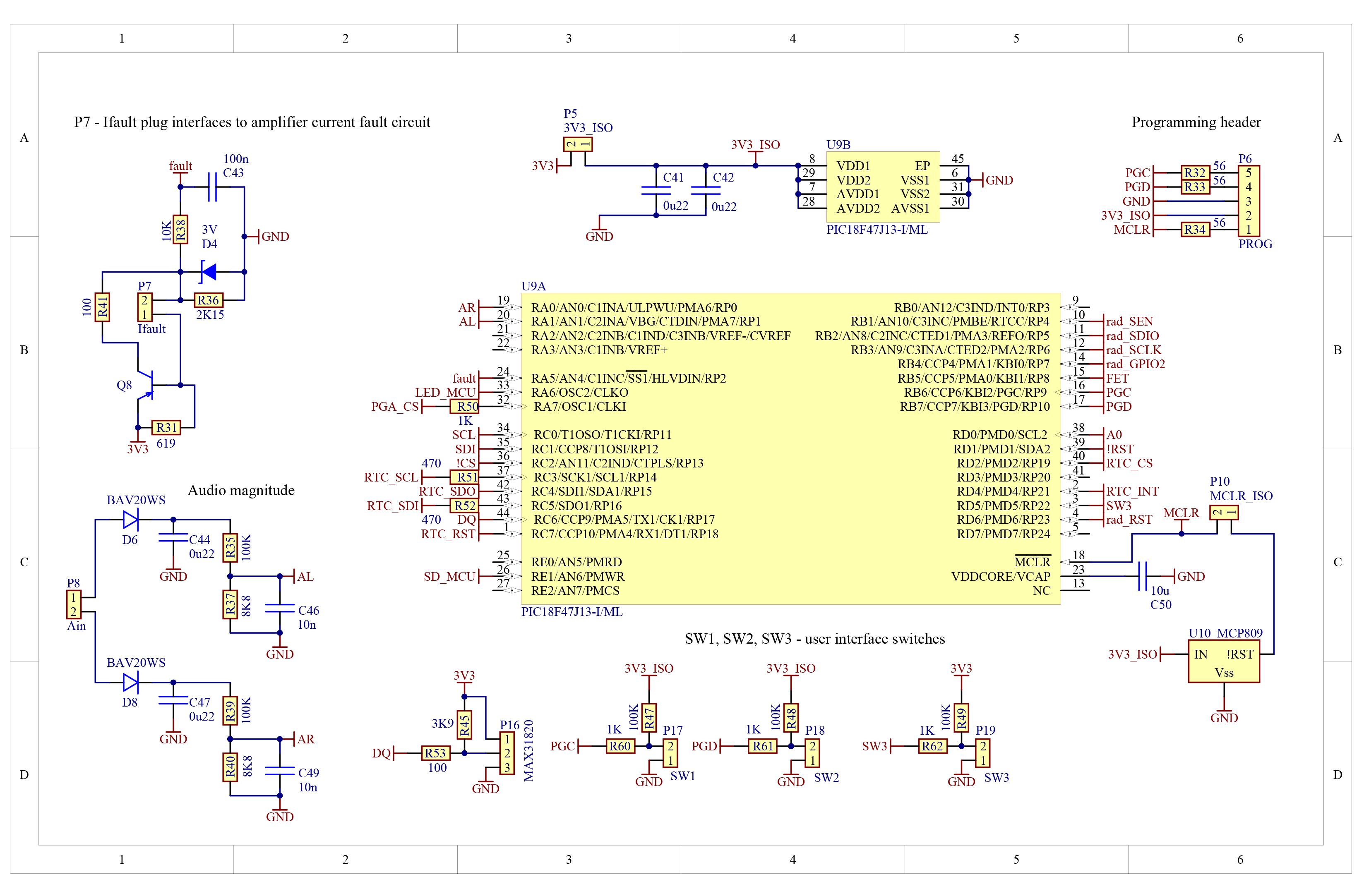
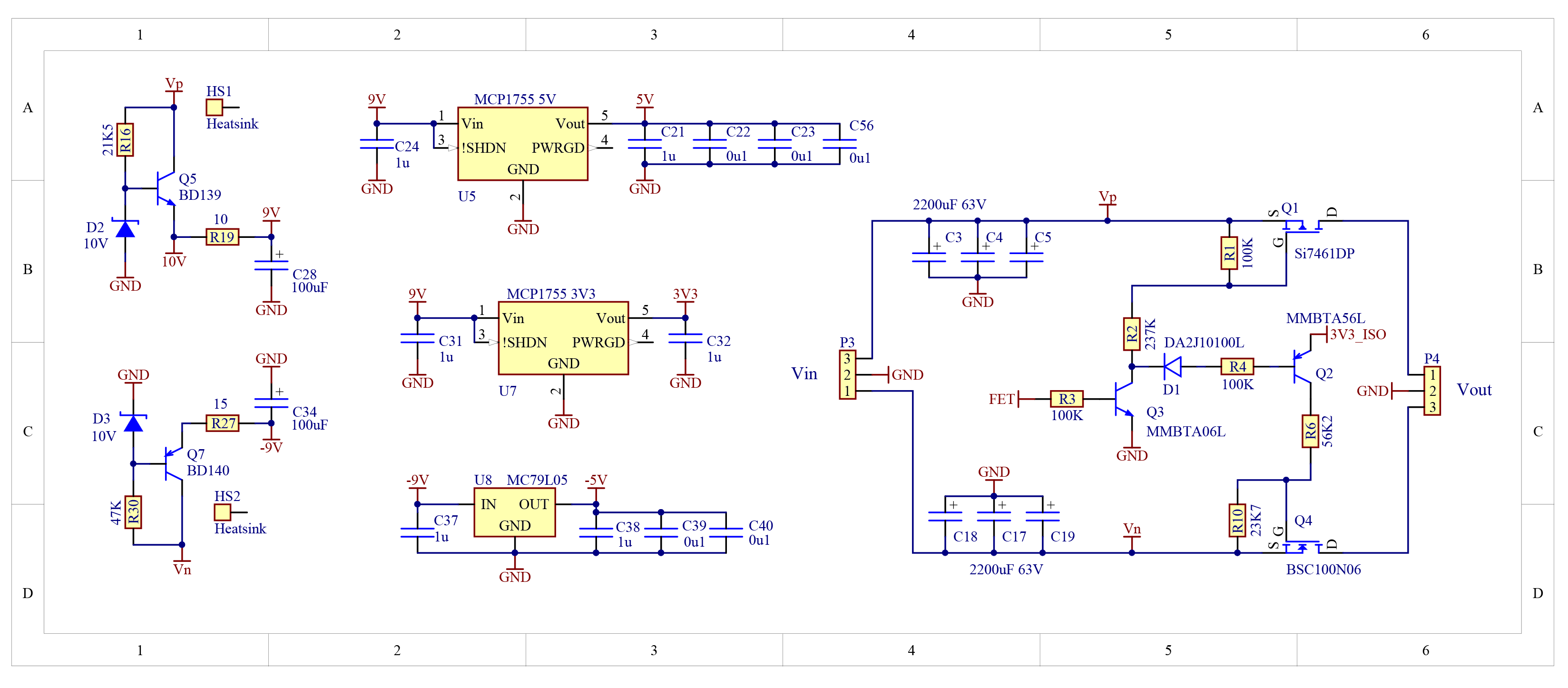
The control board accommodates 3 push button switches for user commands. Two of these switches generate a low-priority interrupt, while the 3rd switch is polled while the MCU is actively responding to user commands when the low-priority interrupt occurs. The control board schematic is shown in figures 19 to 23.
Future work
There are two promising and simple modifications that may improve the amplifier design which are now described. Experimental characterisation of the amplifier indicated that the output stage quiescent current, $I_{O}$, has an excessive dependence on temperature. It is likely that a small modification to the circuit that limits $I_{O}$ will greatly reduce the sensitivity to temperature, namely, the utilisation of a thermistor or similar. A thermistor in close thermal contact with the output transistors can be used to make a temperature dependent modification to the resistance of potentiometer (R46) such that the sensitivity of $I_{O}$ to temperature is reduced.
Two independent constant current sources bias the 2nd differential stage. These two current sources are set approximately equal in magnitude so that the driver stage current is balanced when minimal current is supplied to the 2nd stage input. A more convenient approach replaces one of the current sources with a current mirror such that only a single constant current source is required to bias the 2nd stage.
Appendix
Low-frequency gain
The low-frequency gain of the various stages is calculated and the results are added to obtain the open-loop gain of the amplifier.
The transconductance of the 1st differential stage is,
\begin{equation}
\frac{I_{1}}{2nV_{T}}
\end{equation}
Therefore, the voltage gain of the 1st stage is,
\begin{equation}
\frac{I_{1}}{2nV_{T}}R_{1}
\end{equation}
where $R_{1}$ is the load resistance present on the output of the 1st stage. There are two contributions to the load,
the input of the 2nd stage and the Early voltage of the 1st stage transistor, Q7. Note, the Early voltage of current mirror transistor, Q5 has an insignificant contribution due to its emitter resistor, R7. The impedance due to the Early voltage is,
\begin{equation}
\frac{V_{Early}}{0.5\,I_{1}}
\end{equation}
The Early voltage of Q7 (MMBT6429) is very large, its SPICE model file indicates a value of 804 V, giving a load resistance of,
\begin{equation}
\frac{804}{5\times 10^{-3}} = 1.61\times 10^{5}\,\Omega
\end{equation}
The load resistance due to the 2nd stage input is,
\begin{equation}
(R23+R24)\beta_{Q12}||(R25+R26)\beta_{Q14} = 9.83\times 10^{4}||2.36\times 10^{5} = 6.94\times 10^{4}
\end{equation}
Therefore, the total load resistance on the 1st stage output is,
\begin{equation}
6.94\times 10^{4}||1.61\times 10^{5} = 4.85\times 10^{4}\,\Omega
\end{equation}
The voltage gain of the 1st stage becomes,
\begin{equation}
\left(\frac{2nV_{T}}{I_{1}}+R_{e}\right)^{-1}\times 4.85\times 10^{4} = \left(\frac{0.0537}{0.01}+0.184\right)^{-1}\times 4.85\times 10^{4} = 8.73\times 10^{3}\,V/V
\end{equation}
The transconductance of the 2nd stage is,
\begin{equation}
\frac{1}{68.1+121} = 5.29\times 10^{-3} A/V
\end{equation}
The transconductance of the driver stage is approximately the ratio of the load resistance on the 2nd differential stage output, i.e. the collectors of Q13 and Q15 to the resistance on the emitter of Q19 and Q21 (12$\,\Omega$). A correction to this approximation needs to be made because the dynamic resistance of the LEDs, D6 and D9 are significant.
The dynamic resistance of D6 and D9 are,
\begin{equation}
\frac{nV_{T}}{I} = \frac{9.63\times 0.026}{1.75\times 10^-3} = 143\,\Omega
\end{equation}
The transconductance becomes,
\begin{equation}
\begin{split}
&\frac{1}{12}\left[\frac{1}{1k33} + \frac{1}{1k} + \left[\left[\frac{1}{1k33} + \frac{1}{12\beta_{Q19}}\right]^{-1}+143\right]^{-1}\right]^{-1}
&\times \left[\frac{1}{1k33}+\frac{1}{12\beta_{Q19}} \right]^{-1}/\left[\left[\frac{1}{1k33}+\frac{1}{12\beta_{Q19}} \right]^{-1}+143\right]
\end{split}
\end{equation}
The 1st line is the load resistance divided by 12 and the 2nd line is a voltage divider correction due to the LED dynamics resistance. The datasheet suggests the current gain of Q19 and Q21 $\beta$ are equal to about 200 which gives a driver stage transconductance of 25.9 A/A.
The output stage transresistance when driving an $8\,\Omega$ is simply $8\beta$. For small output voltages, $V_{CE}$ of the output transistors is about 40 V and the current gain is close to 200, therefore, the transresistance is 1600. The total open-loop gain of the amplifier is calculated to be, \begin{equation} 8.73\times 10^{3}\times 5.29\times 10^{-3}\times 2\times 25.9\times 1600 = 131.7\,\textrm{dB} \end{equation} These values can be compared to those listed in table 2 which are derived by simulation.
Thermal dissipation of the output transistors - reactive load
The real power delivered to a linear load driven by a sinusoidal voltage waveform is given by,
\begin{equation}
\frac{1}{T}\int_{0}^{T}dt\,V_{pk}\sin(2\pi t/T)I_{pk}\left[\sqrt{1-\alpha^{2}}\sin(2\pi t/T)+\alpha\cos(2\pi t/T)\right] = \frac{1}{2}V_{pk}I_{pk}\sqrt{1-\alpha^{2}}
\end{equation}
where $V_{pk}$ and $I_{pk}$ is the peak load voltage and current and $T$ is the period of the sinusoidal waveform.
The parameter $\alpha$ takes on values from -1 to 1, representing the fact that the load current may have an arbitrary phase with respect to the load voltage depending on how inductive or capacitive the load is.
The thermal dissipation of each output transistor (ignoring the small contribution of the quiescent current) is given by,
\begin{eqnarray}
P_{th} = \frac{1}{T}\int_{0}^{T/2} V_{supply}I_{pk}\sin(2\pi t/T)\,dt
-\frac{1}{4}V_{pk}I_{pk}\sqrt{1-\alpha^{2}}
\end{eqnarray}
where $V_{supply}$ is the output transistor collector voltage, i.e. the supply voltage. The integral is the power delivered
to both the load and output transistor and the 2nd term is the real power delivered to the load. For a load impedance of Z$\Omega$ the
thermal power dissipated by each output transistor becomes,
\begin{equation}
P_{th} = \frac{V_{supply}}{\pi}\frac{V_{pk}}{Z} - \frac{V^{2}_{pk}}{4Z}\sqrt{1-\alpha^{2}}
\end{equation}
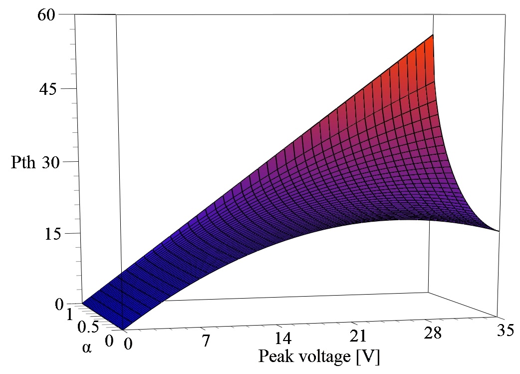
Fig. 26 is a plot of the thermal power dissipated by each output transistor for $V_{supply} = 40V$ and $Z=8\,\Omega$. The maximum power dissipated for $\alpha=0$ is about 20 W, which increases to 55 W for $\alpha=1$.